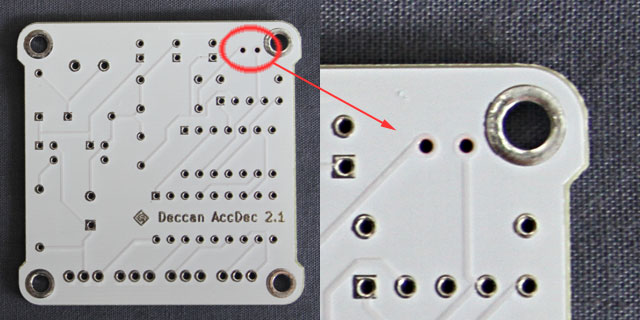
As mentioned in a previous blog, the PCB I designed and ordered from Itead arrived and I started assembling it. Once I got going, I discovered a few problems. Itead did its job immaculately but I managed to make quite a few mistakes - some big, some small. Some involved just fixing the design, some involved tweaking the KiCAD library. I am continuing to test the board and am likely to find a few more. Once all the circuit bugs are ironed out, I can order a fresh set.
One of the great things about KiCAD is all its files are in text format. This allows me to look at and fix things without trying to find a parameter in a dialog box.

One of the great things about KiCAD is all its files are in text format. This allows me to look at and fix things without trying to find a parameter in a dialog box.
Power connections to 16F1823
A few decades ago, I had to design a Dynamic RAM interface for a Z80. I had 20 pages of timing diagrams and calculations but the damn thing would not work and I could not figure out why. It took a while but I finally found out that the MOS chips had their power connections swapped – pin 7 was 5V and pin 14 was ground. Having used TTL most of the time, I could never figure out Vss/Vdd. The same problem came back to bite me. I had the Vss and Vdd connections mixed up. I guess you can’t teach an old dog old tricks either. A bit of PCB surgery and I had it fixed. This is something to fix in the next version of the board.Incorrect solder mask for through-hole LED
The libraries that come with KiCAD may have a few pitfalls. I don't know how old the libraries I have are but I came across a problem with the LED. There was no clearance on the solder mask on the copper side. The pads for the LED were there on the copper side but were completely covered by the solder mask. This meant soldering it was a pain. Turns out the LED shares the file with several SMD versions and the mask on the LED pins were only on one side. You can fix it using the module editor or just hack the text file.Drill size for 2.54mm pitch PCB Terminals
I use 2.54mm pitch PCB Terminals for the turnout motor connections. With four turnout motors to be driven, 12 terminals are required. A 2.54mm pitch terminal is a bit harder to find and a little more expensive but the compactness is more than worth it. According to the datasheet, the lead size is 0.5x0.8mm or 0.94mm dia. The KiCAD file had a drill diameter value of 460 - this 46mils or 1.17mm. The extra clearance of 0.2mm should be fine. In actual fact, it turned out to be rather wobbly – I should have measured the actual lead and opted for a pushfit clearance of 0 or less. The holes I used for the DIP of 320 (32mils or 0.8mm) seem to be a better fit for the connector. The original drill size of 46mils can be seen in the extract below. I simply changed them all to 320 directly in the text file. This is easier to check and fix in the text file.$PAD
Sh "2" C 800 800 0 0 0
Dr 460 0 0
At STD N 00E0FFFF
Ne 2 "/Vmotor"
Po 0 0
$EndPAD
Checking the PCB Legend Consistency
While you can’t be too careful with drill hole sizes, writing a java program to check the legend sizes is probably going a bit too far. Which is what I did. I used it to directly read the text file, check for the following standards and prompt for change. A fixed text file is then written and can be used to replace the original.- All component designations like U1, etc are 40x40mils and 6mils thick. It is visible and in italics.
T0 4400 -2200 400 400 1800 60 N V 21 I "U4"
T1 2400 -2200 400 400 1800 60 N V 21 N "ULN2803"
DS -5000 -500 -4500 -500 80 21
DS -4500 -500 -4500 500 80 21
No comments:
Post a Comment